Micro XRF Measures Smallest Features in Wafers, Microelectronics
Micro XRF Measures Smallest Features in Wafers, Microelectronics
Bowman has added a new precision XRF instrument to its line of instruments used in the PCB, semiconductor, and microelectronics industries.
The Bowman A Series Micro XRF measures the smallest features on semiconductors and microelectronics in a matter of seconds. It can handle very large PCB panels as well as wafers of any size, allowing for full sample coverage and multi-point programmable automation.
Poly-capillary optics focus the X-ray beam to 7.5 µm FWHM, the world's smallest for XRF coating thickness analysis. A 140X magnification camera measures features on that scale; a secondary, low magnification camera provides live-viewing of samples and "birds-eye" macro-view imaging.
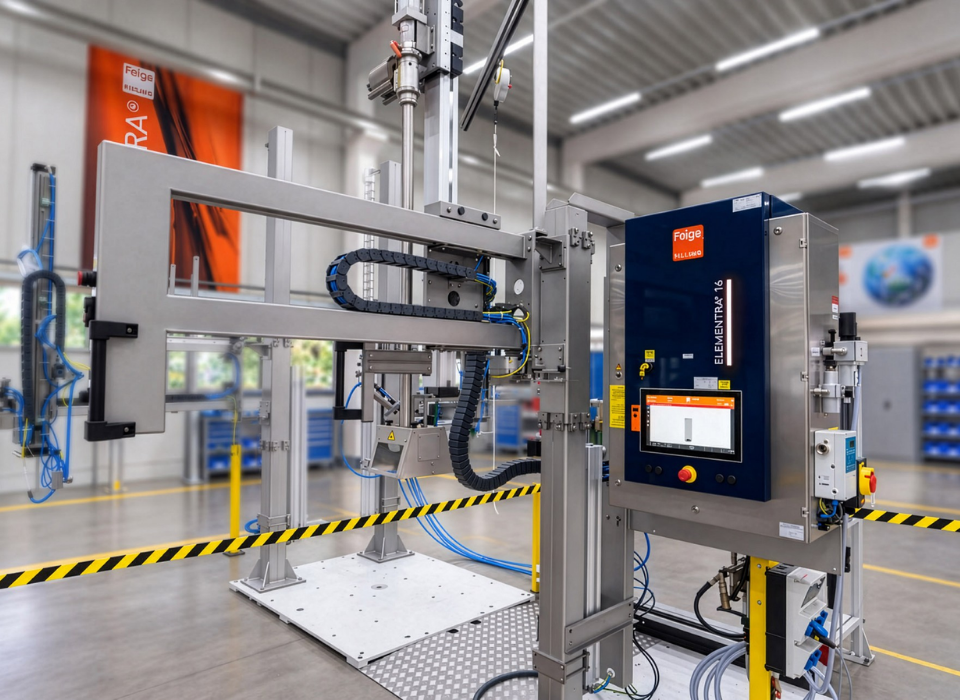
[caption id="attachment_141735" align="aligncenter"] Rendering of A Series for Incorporation with Automated Wafer Handler[/caption]
Bowman's proprietary dual-camera system lets operators see the entire part, click the image to zoom with the high-mag camera, and quickly identify the feature of interest.
A programmable X-Y stage with movement of 23.6 in (600 mm) in each direction can handle the largest samples in the industry. The stage has precision down to +/- 1 µm for each axis, and is used to select and measure multiple points; Bowman pattern recognition software and auto-focus features also do this automatically.
The system's 3D mapping capability can be used to view the topography of ENIG, ENEPIG, EPIG and other elite processes.
A Series instruments include 7.5 µm optics with molybdenum anode tube (chromium and tungsten also available) and a high-resolution, large-window Silicon Drift Detector (SDD) which processes more than 2 million counts per second.
SDDs are the standard, industry-wide, for complex thin films. The high count rate capability is key to achieving a low minimum detection limit (MDL) and highest spectral resolution.
A Series systems are distinctive in that they are cleanroom-ready, have the largest semiconductor stage movement on the market, and are supported worldwide by a service network that provides same-day response for every benchtop XRF requirement.
Equipment evaluation, selection, commissioning, maintenance and modernization is available for users of Bowman instruments, as well as other major XRF brands.
Note: Content may be edited for style and length.
Source
Advertisement
Ad Space728 × 90